- 您现在的位置:买卖IC网 > Sheet目录3851 > PIC16F88-I/ML (Microchip Technology)IC MCU FLASH 4KX14 EEPROM 28QFN
112
8008H–AVR–04/11
ATtiny48/88
Modes of operation supported by the Timer/Counter unit are: Normal mode (counter), Clear
Timer on Compare match (CTC) mode, and three types of Pulse Width Modulation (PWM)
12.11.2
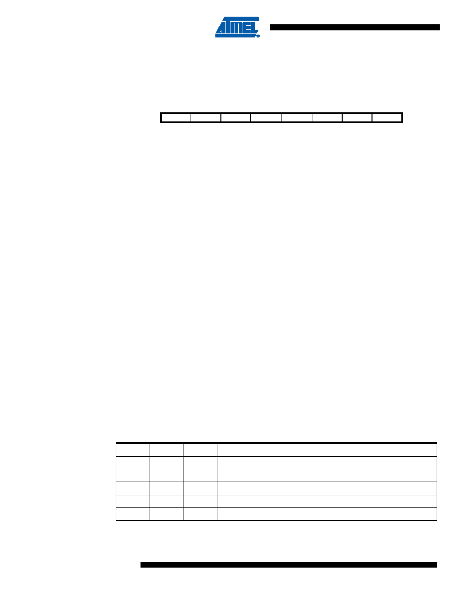
TCCR1B – Timer/Counter1 Control Register B
Bit 7 – ICNC1: Input Capture Noise Canceler
Setting this bit (to one) activates the Input Capture Noise Canceler. When the noise canceler is
activated, the input from the Input Capture pin (ICP1) is filtered. The filter function requires four
successive equal valued samples of the ICP1 pin for changing its output. The Input Capture is
therefore delayed by four oscillator cycles when the noise canceler is enabled.
Bit 6 – ICES1: Input Capture Edge Select
This bit selects which edge on the Input Capture pin (ICP1) that is used to trigger a capture
event. When the ICES1 bit is written to zero, a falling (negative) edge is used as trigger, and
when the ICES1 bit is written to one, a rising (positive) edge will trigger the capture.
When a capture is triggered according to the ICES1 setting, the counter value is copied into the
Input Capture Register (ICR1). The event will also set the Input Capture Flag (ICF1), and this
can be used to cause an Input Capture Interrupt, if this interrupt is enabled.
When the ICR1 is used as TOP value (see description of the WGM1[3:0] bits located in the
TCCR1A and the TCCR1B Register), the ICP1 is disconnected and consequently the Input Cap-
ture function is disabled.
Bit 5 – Reserved Bit
This bit is reserved for future use. For ensuring compatibility with future devices, this bit must be
written to zero when TCCR1B is written.
Bits 4:3 – WGM1[3:2]: Waveform Generation Mode
See TCCR1A Register description.
Bits 2:0 – CS1[2:0]: Clock Select
The three Clock Select bits select the clock source to be used by the Timer/Counter, see Figure
12-10 and Figure 12-11.
Bit
7
6
5
4
3
2
1
0
ICNC1
ICES1
–
WGM13
WGM12
CS12
CS11
CS10
TCCR1B
Read/Write
R/W
R
R/W
Initial Value
0
Table 12-6.
Clock Select Bit Description
CS12
CS11
CS10
Description
0
No clock source (Timer/Counter stopped).
00
1
clk
I/O/1 (No prescaling)
01
0
clk
I/O/8 (From prescaler)
01
1
clkI/O/64 (From prescaler)
10
0
clk
I/O/256 (From prescaler)
发布紧急采购,3分钟左右您将得到回复。
相关PDF资料
PIC18F26J53-I/ML
IC PIC MCU 64KB FLASH 28QFN
PIC18F46K80-I/ML
MCU PIC 64KB FLASH 44QFN
PIC32MX130F064D-I/TL
IC MCU 32BIT 64KB FLASH 44-VTLA
PIC32MX130F064D-I/ML
IC MCU 32BIT 64KB FLASH 44-QFN
PIC18LF46K80-I/ML
MCU PIC ECAN 64KB FLASH 44QFN
AT89S51-24JI
IC 8051 MCU 4K FLASH 44PLCC
AT89S51-24JC
IC 8051 MCU 4K FLASH 44PLCC
AT89S51-24AI
IC 8051 MCU 4K FLASH 44TQFP
相关代理商/技术参数
PIC16F88-I/ML
制造商:Microchip Technology Inc 功能描述:8BIT FLASH MCU SMD 16F88 QFN-28
PIC16F88-I/P
功能描述:8位微控制器 -MCU 7KB 368 RAM 16 I/O RoHS:否 制造商:Silicon Labs 核心:8051 处理器系列:C8051F39x 数据总线宽度:8 bit 最大时钟频率:50 MHz 程序存储器大小:16 KB 数据 RAM 大小:1 KB 片上 ADC:Yes 工作电源电压:1.8 V to 3.6 V 工作温度范围:- 40 C to + 105 C 封装 / 箱体:QFN-20 安装风格:SMD/SMT
PIC16F88-I/P
制造商:Microchip Technology Inc 功能描述:IC 8BIT FLASH MCU 16F88 DIP18
PIC16F88-I/SL
制造商:Microchip Technology Inc 功能描述:
PIC16F88-I/SO
功能描述:8位微控制器 -MCU 7KB 368 RAM 16 I/O RoHS:否 制造商:Silicon Labs 核心:8051 处理器系列:C8051F39x 数据总线宽度:8 bit 最大时钟频率:50 MHz 程序存储器大小:16 KB 数据 RAM 大小:1 KB 片上 ADC:Yes 工作电源电压:1.8 V to 3.6 V 工作温度范围:- 40 C to + 105 C 封装 / 箱体:QFN-20 安装风格:SMD/SMT
PIC16F88-I/SO
制造商:Microchip Technology Inc 功能描述:8BIT FLASH MCU SMD 16F88 SOIC18
PIC16F88-I/SOG
功能描述:8位微控制器 -MCU 7KB 368 RAM 16 I/O Lead Free Package RoHS:否 制造商:Silicon Labs 核心:8051 处理器系列:C8051F39x 数据总线宽度:8 bit 最大时钟频率:50 MHz 程序存储器大小:16 KB 数据 RAM 大小:1 KB 片上 ADC:Yes 工作电源电压:1.8 V to 3.6 V 工作温度范围:- 40 C to + 105 C 封装 / 箱体:QFN-20 安装风格:SMD/SMT
PIC16F88-I/SS
功能描述:8位微控制器 -MCU 7KB 368 RAM 16 I/O RoHS:否 制造商:Silicon Labs 核心:8051 处理器系列:C8051F39x 数据总线宽度:8 bit 最大时钟频率:50 MHz 程序存储器大小:16 KB 数据 RAM 大小:1 KB 片上 ADC:Yes 工作电源电压:1.8 V to 3.6 V 工作温度范围:- 40 C to + 105 C 封装 / 箱体:QFN-20 安装风格:SMD/SMT